| Categories | High Layer PCB |
|---|---|
| Impedance Control: | Yes |
| Copper Thickness: | 1/3 Oz To 2 Oz |
| Silkscreen Color: | White, Black, Yellow |
| Board Thickness: | 0.2mm To 6.0mm |
| Layer Count: | High Layer |
| Min. Solder Mask Clearance: | 0.1mm |
| Min. Line Width/Spacing: | 3mil/3mil |
| Material: | FR-4 |
| Company Info. |
| Shenzhen Benqiang Circuits Co,Ltd. |
| Verified Supplier |
| View Contact Details |
| Product List |
| Technical Parameters | Options |
|---|---|
| Lead Time | 3-5 Days |
| Surface Finish | HASL, ENIG, OSP, Immersion Silver, Immersion Tin |
| Material | FR-4 |
| Min. Solder Mask Clearance | 0.1mm |
| Silkscreen Color | White, Black, Yellow |
| Impedance Control | Yes |
| Min. Hole Size | 0.2mm |
| Layer Count | High Layer |
| Copper Thickness | 1/3 Oz To 2 Oz |
| Solder Mask Color | Green, Blue, Black, Red, Yellow, White |
| Key Words | High Layer PCB Board, High Layer Multi-level PCB, High Layer Printed Wiring Board |
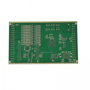
High Layer PCB, also known as High Layer Multilayer PCB, High Layer PCB Board, High Layer Printed Circuit Board or High Layer Circuit Board, is a type of printed circuit board (PCB) with a high layer count. It is widely used in various electronic applications due to its superior design and functionality.
High Layer PCB comes in a variety of silkscreen colors including white, black, and yellow. The silkscreen layer is used to print component designators, logos, symbols, and other important information on the board. The choice of color depends on the customer's preference and the application of the PCB.
The layer count of High Layer PCB usually ranges from 8 to 40, or even more. This high layer count allows for more complex circuit designs and enables the integration of multiple functions into a single board. This makes High Layer PCB an ideal choice for high-performance and densely populated electronic devices.
The board thickness of High Layer PCB ranges from 0.2mm to 6.0mm, depending on the number of layers and the application requirements. The thickness of the board affects its rigidity and flexibility, and it is carefully chosen based on the specific needs of the electronic device.
High Layer PCB is compliant with the Restriction of Hazardous Substances (ROHS) directive, which restricts the use of certain hazardous materials in electronic products. This makes High Layer PCB a safe and environmentally-friendly option for various electronic applications.
The minimum silkscreen clearance of High Layer PCB is 0.15mm, which ensures the clear and accurate printing of all necessary information on the board. This allows for easy identification and assembly of components, resulting in a more efficient production process.
High Layer PCB has a wide range of applications in the electronic industry. Some of the common applications include:
With its high layer count, superior design, and compliance with industry standards, High Layer PCB is a reliable and efficient solution for various electronic applications. It provides a stable platform for the integration of complex circuits, leading to faster and more reliable electronic devices.
Our High Layer PCB offers high density interconnect and advanced functionality for your electronic projects. With our customization service, you can have your High Layer PCB tailored to your specific needs.
We understand the importance of prompt delivery for your projects. That's why our High Layer PCB customization service has a lead time of only 3-5 days. This ensures that you can receive your customized PCBs in a timely manner.
Our High Layer PCB is compliant with RoHS regulations, ensuring that it is environmentally friendly and safe for use in your projects.
We offer a variety of silkscreen color options for your High Layer PCB, including white, black, and yellow. This allows you to choose the color that best suits your design and branding needs.
Our High Layer PCB can be customized with a copper thickness ranging from 1/3 oz to 2 oz. This ensures that your PCB can handle the specific demands of your project.
To meet the different needs of our customers, we offer a range of surface finish options for our High Layer PCB, including HASL, ENIG, OSP, immersion silver, and immersion tin. This allows you to choose the surface finish that best suits your project requirements.
With our High Layer PCB customization service, you can be sure that you will receive a high-quality and tailored PCB for your project. Contact us now to get started.
Our High Layer PCB product is carefully packaged and shipped to ensure safe delivery to our customers.
Each High Layer PCB is individually wrapped in anti-static packaging to protect against electrostatic discharge during transportation. The wrapped PCBs are then placed in a sturdy cardboard box, with additional padding and cushioning materials, to prevent any damage during transit.
For larger orders, we use pallets to securely pack the PCBs. Each pallet is shrink-wrapped and labeled with the product and shipping information for easy identification and handling.
We offer various shipping options to accommodate our customers' needs and preferences. Our standard shipping methods include air freight and sea freight, with tracking information provided for all orders.
We also offer expedited shipping for urgent orders, with additional charges applied. Our team works closely with trusted shipping partners to ensure timely and reliable delivery of our products.
For international orders, customers are responsible for any applicable customs and duties fees. We provide all necessary documentation for smooth customs clearance, and our team is available to assist with any inquiries or issues that may arise.
Thank you for choosing our High Layer PCB product. We are committed to providing the best packaging and shipping services to ensure your satisfaction. For any further questions or concerns, please do not hesitate to contact us.

|