| Sign In | Join Free | My ecer.com.ru |
|
| Sign In | Join Free | My ecer.com.ru |
|
| Categories | LiNbO3 Wafer |
|---|---|
| Brand Name: | BonTek |
| Model Number: | Lithium Niobate (LiNbO3) |
| Certification: | ISO:9001, ISO:14001 |
| Place of Origin: | China |
| MOQ: | 2 pcs |
| Price: | Negotiable |
| Payment Terms: | T/T |
| Supply Ability: | 10000 pcs/Month |
| Delivery Time: | 1-4 weeks |
| Packaging Details: | Cassette/ Jar package, vaccum sealed |
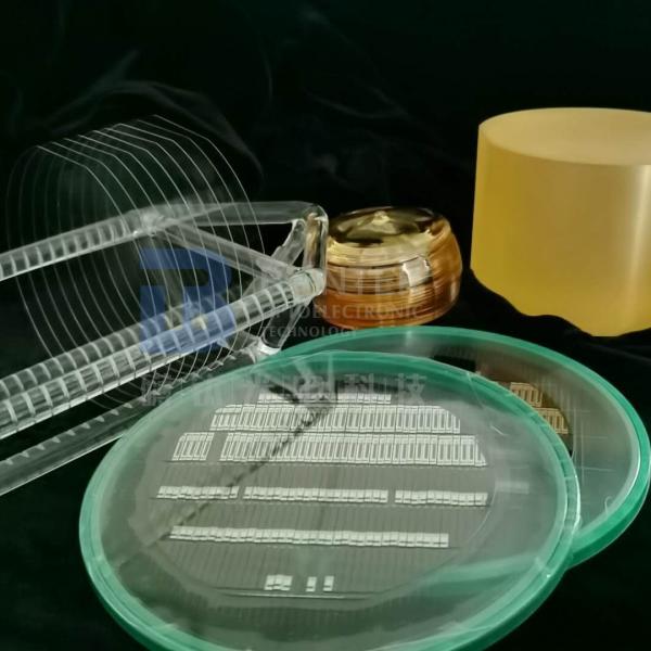
| Product: | LiNbO3 Wafer |
| Grade: | SAW and Optical |
| Diameter: | 3inch, 4inch, 6inch, 8 inch |
| Orientation: | X-cut, Z-cut, Y-cut, 128Y-cut |
| Thickness: | 0.35mm, 0.5mm, 1mm |
| Surface: | DSP, SSP |
| Roughness: | Ra<1nm |
| Application: | SAW Devices, Optical Waveguides |
| Company Info. |
| Hangzhou Freqcontrol Electronic Technology Ltd. |
| Verified Supplier |
| View Contact Details |
| Product List |
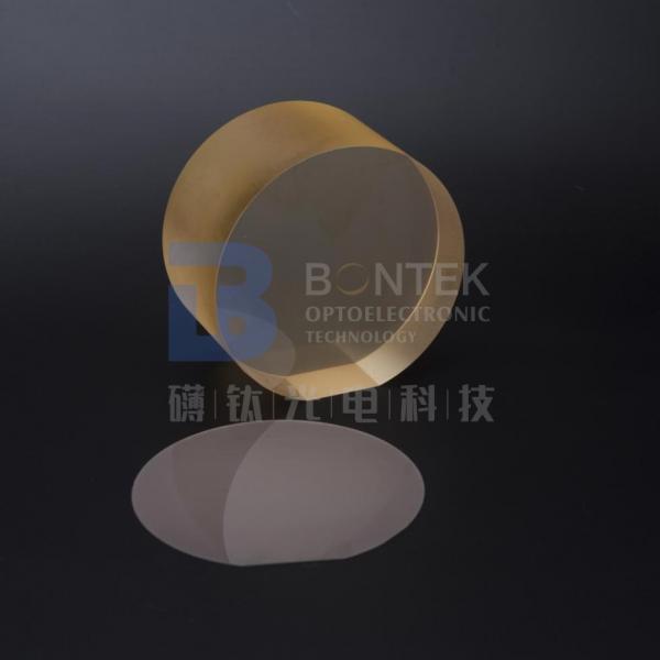
Ferroelectric LiNbO3 wafers of different Orientations For SAW Devices Optical Waveguides
Lithium Niobate (LN) is a ferroelectric material with excellent electro-optic, nonlinear, and piezoelectric properties. Lithium niobate crystals are important materials for optical waveguides, mobile phones, piezoelectric sensors, optical modulators and various other linear and non-linear optical applications.
The largest use of Lithium Niobate (LN) is in SAW devices used in telecommunication devices. When voice communication and data communication are performed, SAW devices such as SAW filters and SAW duplexers are mounted in communication devices as filters for preventing noise and interference. Lithium Niobate (LN) crystals are also used in optical applications.

Material | 3" 4" 6" 8" LN wafer Saw/Optical grade |
Orientation | X/Z/Y41°/Y64°/Y128°/YZ/YX or Customized |
Curie Temp | 1142°C±3°C |
Doped with | Zn, MgO single or double doped available |
Surface finish | single or double sides polish (DLP/SLP/ SSP/DSP all available) |
Thickness | 0.18/0.25/0.35/0.50/1.00 + mm |
TTV | < 1~5µm |
BOW | ± (25µm ~40um ) |
Warp | <= 35µm |
LTV (5mmx5mm) | <1.5 um |
PLTV(<0.5um) | ≥98% (5mm*5mm) with 2mm edge excluded |
Edge | Compl't with SEMI M1.2@with GC800# .regular at C typed |
Orientation flats | available, per request |
Polished side Ra | Roughness Ra<=5A |
Back Side Criteria | Roughness Ra:0.5-1.0µm GC#1000 |
Edge Rounding | Compliant with SEMI M1.2 Standard/refer to IEC62276 |
Cracks, saw marks, stains | None |

FAQs:
A: We look at ourselves as the piezo wafer specialist. We are the very first to work with Single Crystal Quartz in China about 30 years ago. Then gradually we step in the field of LiNbO3, LiTaO3, Quartz glass, LGS, CTGS etc. Especially, if you are looking for a piezo quartz supplier, we are the ultimate choice! We export millions of quartz blanks each year because we master the AT, SC and IT cuts with superior angle precision.
A: Yes, of course. We can fabricate as per your request. In addition, we are so experienced with piezo wafers that we can provide you relevant suggestions if you are not 100% sure about your choice. Besides, we do have some standard wafers in stock, please check with us.
A: Yes, we would suggest you go with the courier agent you are most familiar with (DHL, FedEX, UPS etc.). We can ship via your account. And, of course, we will pack the products safely in acceptable size to help you save the shipping cost. If you need us to take care of the freight, it’s also not a problem. We also have good discount with the international courier companies.
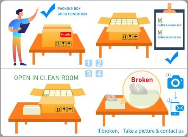
A: The wafer products are fragile and sometimes expensive. The last thing, as the manufacturer, we want to see is the products we make were damaged during courier. As a result, we will pack the wafers adequately and put them in a proper carton filled with buffer sponge. However, accidents are inevitable sometimes. So, please follow the “Acceptance check” steps shown in the drawings below. If the unwanted happened, we will either give the replenishment or refund if you follow the checking steps.
A: Sure. Factory inspection is important for large quantity purchase and long-term cooperation. Face to face discussion is what we mostly confident with. During the past years, big names around the world have witnessed our progress in factory build-up. These days, due to the Covid-19 pandemic, we also had the experience of videoconferencing with global buyers.
Acceptance Check
|